

Quick answer. Contact resistance in a NEMA photocontrol base is set by three things: the real metal-to-metal contact area, which is far smaller than the surfaces appear; the condition of the contact finish at that interface; and the spring force pressing the two halves together. When any one of them degrades, resistance rises, and because the power dissipated at the interface follows P = I²R, a resistance increase of a few milliohms can turn into watts of local heat that accelerates oxidation and drives resistance higher still. Substrate material, plating structure and contact force therefore have to be evaluated together.
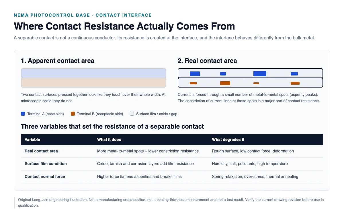
What Is Contact Resistance in a NEMA Photocontrol Base?
A NEMA photocontrol base is a separable electrical interface, not a continuous conductor. The resistance a controller sees between its internal circuit and the luminaire is therefore made of two parts: the bulk resistance of the metal path, which is small and stable, and the resistance of the joint where the base contacts meet the receptacle contacts. The second part is the one that moves.
That joint resistance is usually described as the sum of two mechanisms. Constriction resistance appears because two apparently flat metal surfaces actually touch only at microscopic high points. Current is forced to funnel through those small spots, and the funnel effect adds resistance even though the metal itself is a good conductor. Film resistance appears because most metals carry a surface layer — oxide, sulfide, tarnish, or adsorbed contamination — that is far less conductive than the metal underneath. A tin surface, for example, carries a thin oxide that must be mechanically displaced before good metal-to-metal contact exists.
Both mechanisms respond to the same variable: normal force. Higher contact force flattens the high points, increases the real contact area and helps break through surface films. That is why a contact that measures well when new can measure badly after the spring has relaxed, and why plating quality cannot be judged separately from the spring design behind it.
This is also why contact resistance should never be discussed as a single abstract number. The meaningful question is not only what the initial value is, but what happens to it after mating cycles, after thermal ageing and after environmental exposure. A datasheet that lists a design rating tells you the intended operating envelope; only a measurement record tells you what the interface actually does.
Why Does High Contact Resistance Cause Overheating?
Power dissipated at a contact interface is the product of current squared and interface resistance. Because the dissipation happens in a very small volume — the contact spots — the resulting temperature rise is local and can be much higher than the rise in the surrounding metal. The relationship is quadratic in current, which is the part buyers most often underestimate: doubling the current quadruples the heat at the same resistance.
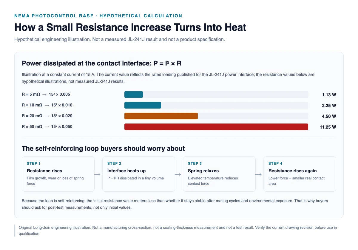
A simple illustration makes the scale visible. At a constant 15 A, 5 mΩ dissipates about 1.1 W at the interface, 10 mΩ about 2.3 W, and 50 mΩ about 11.3 W. These figures are hypothetical and are used only to show the shape of the relationship; they are not measurements of any Long-Join product, and no acceptance limit should be inferred from them. The current value is the rated loading published for the JL-241J power interface, but the resistance values are arbitrary.
The engineering concern is not the one-off wattage. It is the feedback loop that follows. Local heating raises the temperature of the spring contact, and a metal that is held at elevated temperature for long periods loses part of its elastic load. Lower contact force means a smaller real contact area, which means higher resistance, which means more heat. In a sealed luminaire enclosure with limited convection, the loop has no easy escape path. This is why contact resistance and temperature rise are usually evaluated as a pair rather than as independent line items.
A second consequence is often overlooked on control bases: a resistance change affects voltage as well as heat. On a 0–10 V or DALI dimming circuit the current is tiny, so heating is negligible, but a poor interface still introduces an offset and instability into a signal whose whole useful range is a few volts. That is a functional failure, not a thermal one, and it will not show up in a temperature-rise test at rated power current.
What Causes Contact Resistance to Increase?
Insufficient Spring Contact Force
Contact force is the single most important mechanical variable in a separable connection, and it is the one buyers can least easily inspect on a finished part. If the spring is under-dimensioned, over-stressed during assembly, or made from a material that relaxes at operating temperature, the real contact area shrinks and film resistance grows. Force also drops after repeated mating if the contact has been deformed beyond its elastic range. This is why mating durability and contact resistance are normally reviewed together: cycling a contact reveals spring behaviour that a single initial measurement cannot.
Contact Surface Oxidation and Corrosion
Copper alloys oxidise readily. Nickel slows that process, and a noble finish such as gold prevents it at the surface altogether. Where the finish is thin, porous, or absent at the contact spot, the underlying metal reacts with oxygen, humidity, sulfur compounds and chloride. Outdoor luminaires are exposed to all four. The resulting film is thin enough to be invisible and thick enough to matter electrically. Coastal installations and industrial atmospheres accelerate the process, which is why a salt-spray result is often requested alongside contact resistance data.
Plating Wear During Mating Cycles
Every installation and removal cycle slides the two contact surfaces against each other. That sliding wipes the finish at the contact spot. Gold is soft, so a thin gold layer can be worn through to the nickel beneath; nickel then oxidises slowly and resistance climbs. Tin behaves differently: it wears less dramatically but is prone to fretting, where small repetitive movements re-expose fresh metal that oxidises and builds up insulating debris. The number of cycles a design actually sees matters, and so does whether the cycles involve full insertion or partial movement from vibration.
Contamination and Poor Mating Compatibility
Contamination arrives from several directions: residues from plating and cleaning, airborne dust and salt, and debris generated by the contact itself as it wears. Mating compatibility is the other half of the problem. Pairing a gold-finished contact with a tin-finished one is not automatically wrong, but it changes the wear and corrosion behaviour compared with a matched pair, and it can shift the failure mode from wear to galvanic attack in the presence of moisture. Because a photocontrol base is normally mated with a receptacle from a different supplier, this is a genuine system-level variable — not something the base supplier alone controls.
How Do Contact Materials and Plating Affect Reliability?
The materials in a contact system are not interchangeable, and none of them is “best” in isolation. Each is chosen for a function, and the functions only work as a stack.
| Element | Primary function | Why it is used | What can go wrong |
|---|---|---|---|
| Phosphor bronze substrate | Spring force plus conductivity | Good elastic behaviour and fatigue resistance at moderate conductivity, so it holds contact force over many cycles | Stress relaxation at sustained high temperature; loses force if over-stressed on assembly |
| Brass substrate (e.g. H62) | Current carrying with formability | Higher conductivity and lower cost, well suited to power contacts where a separate spring provides the force | Lower spring quality; relies on the surrounding design for contact force |
| Nickel underplate | Diffusion barrier and wear support | Separates the substrate from the noble finish, slows interdiffusion and gives the soft gold a harder base | Too thin or porous defeats the barrier; oxidises if left as the outermost surface |
| Gold finish | Corrosion-free contact surface | Does not form an insulating oxide, so resistance stays low and stable, particularly at low force and low current | Soft and thin coatings wear through; porosity at low thickness exposes nickel |
| Tin finish | Conductive terminal surface | Low cost, well-established in power terminals, good for solderability | Surface oxide requires force and wipe to displace; fretting corrosion in small-movement applications |
The practical reading of this table is that a supplier’s material list is only the starting point. What determines reliability is whether the stack is appropriate to the current level, the contact force and the environment — and whether the process holds that stack consistently from lot to lot. A design that is correct on paper but plated unevenly will fail in the field in ways no drawing reveals.
JL-241J Contact Construction: A Practical Engineering Example
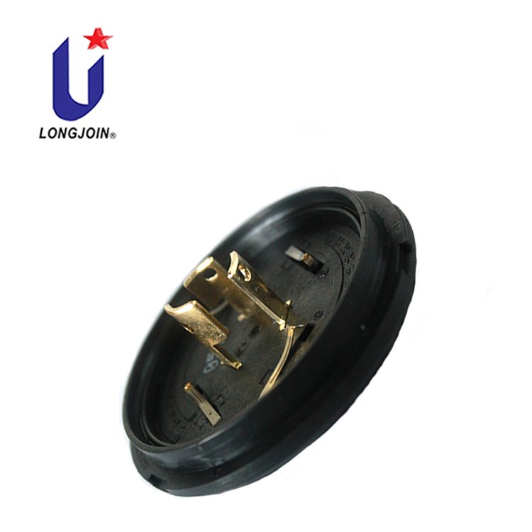
Long-Join’s published documentation for the JL-241J NEMA 7-pin base distinguishes two contact groups, and the distinction matters more than a generic “gold plated contacts” claim would suggest:
- Power contacts: H62 brass substrate.
- Four conductive dimming pins: phosphor bronze substrate, with gold and tin finishes over nickel under-plating.
- Power interface rating: maximum 480 Vac, 50/60 Hz, 15 A rated loading.
- Signal circuit rating: 0–30 Vdc, 250 mA maximum.
Two points follow. First, it is not accurate to describe every contact in the base as phosphor bronze; the power contacts and the dimming pins use different substrates for different reasons, and a buyer comparing quotations should compare like with like. Second, the material statement is a design specification, not a measurement. The manufacturer’s datasheet documents material groups and finish types; it does not publish coating thickness values, contact resistance values or mating-life results for a specific production lot.
That distinction is not a weakness in the documentation — it is the correct boundary. Coating thickness is a process parameter that varies by lot and is verified by measurement, not by a catalogue. A supplier who offers a thickness figure without a measurement record has given you a marketing number, not evidence.
Full documentation is available in the JL-241J 7-pin material datasheet and the electrical assembly specification, revision 2405V2. Product information is on the JL-241J product page.
How Should OEM Buyers Verify Contact Performance?
The verification set below is what a lighting-controller OEM normally needs before approving a base for production. The right-hand column is deliberately written as a buyer decision, because the acceptance criteria should come from the application and the customer specification, not from whatever the supplier happened to test.
| Item to verify | What to request | Why it matters | Buyer decision to record |
|---|---|---|---|
| Initial contact resistance | Measured value per contact, method and test current | Establishes the baseline the design starts from | Your own upper limit for the application, documented before testing |
| Resistance after mating cycles | Values after a defined cycle count, with the mating receptacle identified | Shows whether the finish survives handling and servicing | Cycle count relevant to your installation and service model |
| Resistance after environmental exposure | Values after salt spray, damp heat or thermal cycling as applicable | Reveals corrosion behaviour that initial values hide | Exposure conditions that match your target market |
| Contact force | Design force, and how it is maintained over life | Force drives real contact area and film breakdown | Minimum force you will accept for the mating receptacle used |
| Plating specification | Finish type, substrate, and the drawing revision it applies to | Determines corrosion and wear behaviour | Written confirmation that the revision matches the parts supplied |
| Measurement method | Four-wire (Kelvin) versus two-wire, test current, probe locations | Two-wire measurements include lead and probe resistance and are not comparable | Require four-wire measurement so results can be compared between suppliers |
| Acceptance criteria | The pass/fail limits agreed before the test | A result without a criterion cannot be judged | Sign off the criteria in writing before samples are tested |
One further point on method: a measurement taken with a dry-circuit tester and a measurement taken at rated current are not the same measurement. The first characterises the interface; the second includes the effect of current-induced heating. Ask which was used, and do not compare a dry-circuit figure from one supplier with a loaded figure from another.
Frequently Asked Questions
What causes high contact resistance in a photocontrol base?
Most commonly a combination of three factors: insufficient spring force reducing the real contact area, surface films — oxide, tarnish or contamination — at the interface, and wear of the finish at the contact spot after repeated mating. Contamination introduced during assembly or by the environment makes each of these worse. Because the three interact, a base that measures acceptably when new can still show rising resistance after thermal ageing or after a few dozen mating cycles.
Can gold plating eliminate contact failures?
No. Gold removes one failure mechanism — surface oxidation — because it does not form an insulating oxide. It does not remove wear, contamination, insufficient spring force or mechanical damage. A thin or porous gold layer can be worn or penetrated, exposing the underplate, and a gold surface mated against tin introduces a dissimilar-metal interface that behaves differently from a matched pair. Gold improves the corrosion margin; it does not replace correct spring design and process control.
Why is phosphor bronze used in spring contacts?
Phosphor bronze combines useful electrical conductivity with good elastic behaviour and fatigue resistance, so a formed contact can hold a stable force through many deflection cycles. That combination is why it appears in spring-loaded contact positions rather than in straight current-carrying bars, where a brass with higher conductivity and lower cost is usually the better choice. Its limit is thermal: sustained operation near the upper end of the temperature range gradually relaxes the spring.
How is contact resistance measured?
The standard approach in connector engineering is a four-wire, or Kelvin, measurement: a current is driven through the contact pair and the voltage drop is measured with a separate pair of probes placed as close as possible to the interface, so lead and probe resistance drop out of the result. Test current, probe placement, sample conditioning and the number of samples all affect the number reported, which is why a bare value without method detail cannot be compared across suppliers.
What documents should OEM buyers request?
At minimum: the drawing for the exact configuration, with revision; the material and finish specification; contact resistance data with the method stated; mating durability results with the receptacle identified; temperature rise data if the base will carry power; corrosion test results with the method and duration; and the certification documentation with its scope. Anything not covered by those documents should be recorded as open, not assumed.
Key Takeaways
Contact resistance is created at the interface, not in the metal, and it is governed by real contact area, surface film condition and spring force. Because dissipation follows P = I²R, an increase measured in milliohms becomes meaningful heating, and heating feeds back into spring relaxation. Material choices are functional rather than hierarchical: phosphor bronze for spring positions, brass for power contacts, nickel as a barrier, gold for a stable signal surface, tin for economical power terminals. On the JL-241J, the manufacturer documents H62 brass power contacts and phosphor bronze dimming pins with gold and tin finishes over nickel under-plating — a design specification, not a thickness or test record. Buyers should therefore approve on measured data with a stated method and agreed acceptance criteria, not on a plating description alone.
Request contact material and technical evaluation for JL-241J.
Send us the details that determine the right contact configuration, and our engineering team will respond with the relevant material and finish documentation.
- Product configuration required (pin count, contact arrangement)
- Rated current and voltage of the application
- Target contact resistance and your measurement method
- Application environment (coastal, industrial, temperature range)
- Estimated annual purchase volume
References and Technical Sources
- How to Evaluate the Reliability of a NEMA Photocontrol Base Before Bulk Purchasing — pillar guide covering the full pre-purchase evaluation sequence.
- Long-Join JL-241J NEMA 7-pin material datasheet — contact material groups and finish types.
- Long-Join JL-241J electrical assembly specification, rev. 2405V2 — published design ratings.
- Long-Join JL-241J product page — configuration and ordering information.
- ANSI C136.41-2025 — interface requirements for external locking-type controls and luminaires.



4 Responses